How Europe's Chip Processes Differ

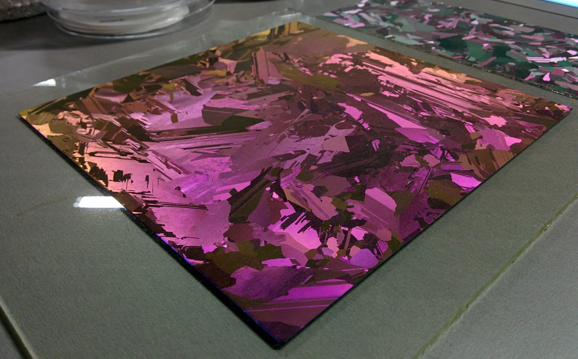
Ten semiconductor manufacturing processes explained, from leading-edge EUV logic to memory Europe no longer makes, with what each optimises for.
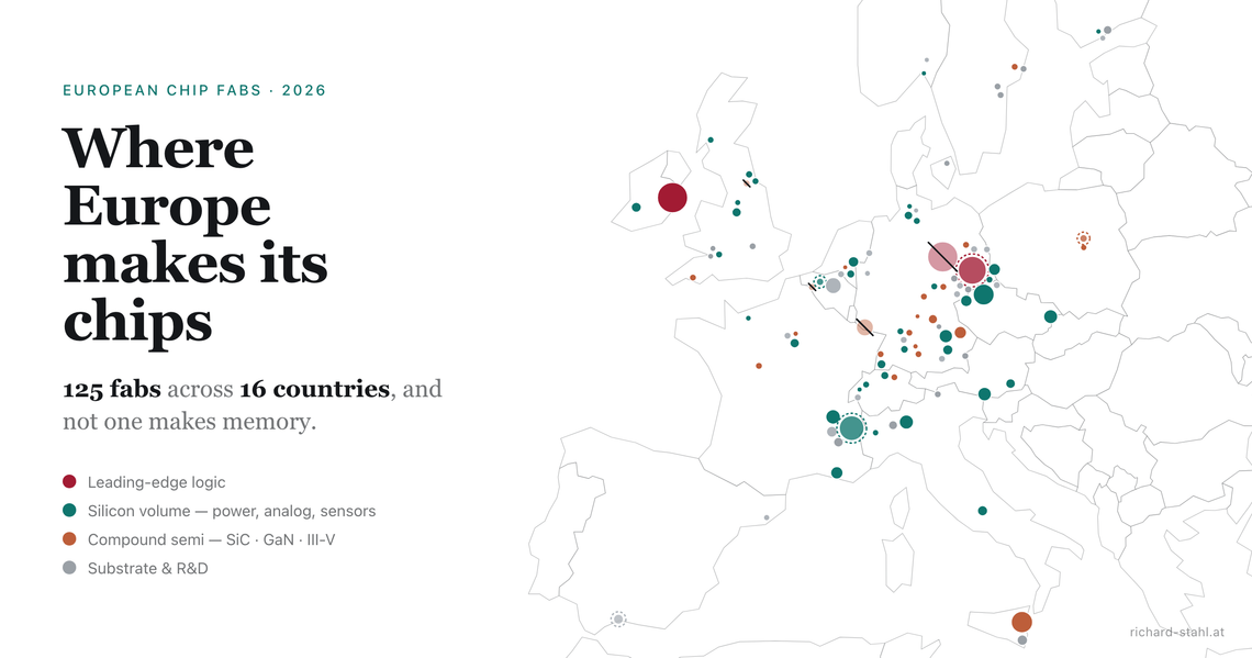
Every fab on the atlas map runs the same basic trick: project a pattern onto a wafer, etch it, deposit a fresh layer, repeat until a circuit stands. What separates the processes is what they optimise for. Logic fabs chase transistor density, power fabs chase volts and amps, MEMS fabs chase moving precision, compound fabs change the crystal itself, and memory fabs, of which Europe has none, chase cost per stored bit. The profiles below take each in turn; the table at the end sums up the differences.
1. Leading-edge logic — Chasing density
The brains of computing: CPUs, GPUs and AI accelerators.
Scale: 16 nm → 2 nm · Light: EUV, 13.5 nm · Wafers: 300mm Fab cost: $20bn+ class; Leixlip ~€17bn · On this map: Intel Leixlip; imec & CEA-Leti (R&D only)
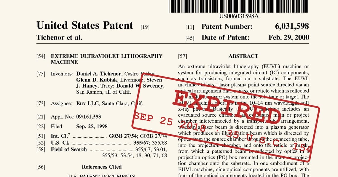
A laser fires at a falling droplet of molten tin, twice, up to 50,000 times a second; the second pulse vaporises the droplet into a plasma that flashes light at a 13.5-nanometre wavelength (extreme ultraviolet, or EUV), far shorter than ordinary light, letting it draw much finer circuit lines. Mirrors, not lenses, focus that light onto the wafer, printing one layer of circuitry the way a stencil prints a street map onto a fingernail. A modern logic chip needs this stencil applied dozens of times, each layer aligned to the last within a few nanometres.
Only three companies run this process at volume: TSMC, Samsung and Intel. Each EUV scanner costs on the order of $180 million to $380 million, and ASML is the sole manufacturer of the tool, so entry requires several billion dollars just for lithography before land, cleanrooms and other equipment are added. Europe has exactly one production-scale leading-edge fab: Intel's Fab 34 in Leixlip, an Intel 3, EUV-based €17 billion plant that opened in 2023. Elsewhere in Europe, sub-10-nanometre work exists only as research: pilot lines at imec in Leuven and CEA-Leti in Grenoble, not production.
ASML is the sole builder of EUV scanners: twin laser pulses hit a tin droplet up to 50,000 times a second to generate 13.5nm light.
2. Mature logic — Chasing cost per chip
The small processors that run cars, factories and appliances.
Scale: 28 nm and older · Light: DUV, 193 nm · Wafers: 200 / 300mm Fab cost: a fraction of leading-edge; tools long paid off · On this map: X-FAB, LFoundry Avezzano, TI Freising, Intel Fab 24
Mature logic uses the same print-etch-repeat cycle as leading-edge chips, but with deep-ultraviolet light at a 193-nanometre wavelength instead of EUV, light roughly fourteen times longer, focused through lenses rather than mirrors. The tools were designed years ago, are long since paid for, and cost a fraction of an EUV scanner: tens of millions of dollars rather than hundreds of millions. Because a car's window-lift motor or a washing machine's control chip doesn't need billions of transistors packed onto a fingernail, the coarser, cheaper stencil is enough, and it can run for decades without buying anything new.
Mature nodes trade density for cost and certainty. A DUV scanner runs tens of millions of dollars against $180 million or more for EUV, and the process, largely unchanged for a decade, is already qualified against automotive and industrial reliability standards that leading-edge nodes have not yet earned. Density is not the point: a control chip inside an airbag or a thermostat must work the same way for fifteen years, not chase the newest benchmark. Much of Europe's chip output by wafer volume sits at 28 nanometres or older, on lines that would be obsolete for a phone processor but suit a car well.
DUV lithography tools cost roughly $30m–$60m each, a third to a sixth the price of an EUV scanner ($180m–$380m).
Sources: 1
3. FD-SOI — Chasing power efficiency
Low-power logic and radio on one die; a European invention.
Scale: 18–28 nm · Light: DUV, 193 nm · Wafers: 300mm, on Soitec SOI Fab cost: no EUV needed; standard DUV lines · On this map: GF Dresden, ST Crolles; Soitec Bernin (wafers)
FD-SOI starts from a different kind of wafer, made by Soitec in Bernin, near Grenoble: a thin film of silicon, so thin the transistor's channel is fully depleted of charge, sits atop a buried layer of insulating oxide, and the foundry builds ordinary flat transistors on top of that stack using standard DUV lithography. The insulating layer underneath lets engineers apply a small voltage from the back side, a back-bias, that pushes each transistor's switching threshold up or down like a dimmer switch: one direction trades power for raw speed, the other trades speed for near-idle power draw, chip by chip or block by block.
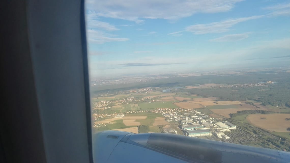
FD-SOI is largely a European process. CEA-Leti in Grenoble developed the underlying transistor architecture, and Soitec, a few kilometres away in Bernin, is the main supplier of the specialty wafers it requires; GlobalFoundries runs it at volume in Dresden (22FDX) and STMicroelectronics runs 28 and 18-nanometre versions in Crolles. Compared with FinFET logic, FD-SOI packs in fewer transistors per square millimetre, but its insulated channel is naturally suited to mixing radio circuitry onto the same die and holds up better against the radiation that damages ordinary silicon in orbit.
GlobalFoundries' Dresden fab runs 22nm FD-SOI at about 950,000 300mm-equivalent wafers a year, on Soitec substrates from Bernin, France.
Sources: 1
4. BCD / smart power — Chasing integration
One chip that senses, decides and switches high voltage.
Scale: 40 nm–0.6 µm class · Light: DUV / i-line · Wafers: 200 / 300mm Fab cost: Infineon's Dresden smart-power fab: €5bn · On this map: ST Agrate & Rousset, ams OSRAM Premstaetten
BCD packs three different transistor families onto one chip: bipolar transistors that sense small analog signals, CMOS logic that decides what to do, and DMOS power transistors that switch the current a motor or battery actually needs. The name is literal, Bipolar-CMOS-DMOS. STMicroelectronics (then SGS) invented it in the mid-1980s; its first product, the 1985 L6202 motor-driver chip, switched 60V at 5A while also containing digital control logic, a combination no single process had managed before.
BCD does not chase smaller transistors the way logic chips do. Precision analog needs physically larger devices to control noise and matching, and the DMOS power transistor needs a wide, lightly doped region to block voltage without breaking down; even TSMC's BCD line still runs from 0.6 micron down to 40 nanometres, nowhere near the leading edge. That ceiling is why plants like ST's Agrate Brianza, running roughly 90-nanometre BCD, stay commercially relevant for decades instead of being retired for something denser. Discrete power chips push further still, trading integration for raw voltage and current.
STMicroelectronics invented BCD in 1985; its first chip, the L6202, switched 60V at 5A while carrying its own control logic.
5. Silicon power — Chasing voltage
Stand-alone high-voltage switches: MOSFETs and IGBTs.
Scale: volts & microns, not nm · Light: coarse litho + backside grinding · Wafers: 150–300mm, thinned to ~20 µm Fab cost: Villach 300mm line: €1.6bn · On this map: Infineon Villach & Dresden, Nexperia, Vishay, Bosch
Discrete power chips don't switch by shrinking transistors sideways; current flows vertically, entering one face of the wafer and exiting the other through a thick, lightly doped layer that holds off the blocking voltage. Thickness and purity of silicon replace feature size as the real craft, so finished wafers are ground down from the back to a few tens of microns. A MOSFET switches fast at lower voltages; an IGBT trades some speed for handling far higher voltage and current.
Discrete power chips are rated in volts and amps, not nanometres. Ordinary MOSFETs cover roughly 20 to 900 volts for chargers, solar inverters and car electronics; IGBTs take over above a few hundred volts and scale up to 6,500-volt parts used in trains, HVDC links and grid converters. This is a segment Europe still leads: Infineon, STMicroelectronics, onsemi, Nexperia, Vishay and Bosch all run silicon power lines here. Plain silicon has a ceiling, though; above roughly 1,200 volts, newer silicon-carbide devices increasingly take the highest-voltage, highest-efficiency designs.
Infineon's €1.6bn Villach fab thins 300mm power wafers to about 20 micrometres, roughly a third the thickness of a human hair.
Source: fab records on this map
6. MEMS & sensors — Chasing moving precision
Chips with moving parts: motion, sound and pressure.
Scale: 1–20 µm moving parts · Light: mature litho + deep etch (DRIE) · Wafers: 150–200mm Fab cost: low; decades-old tools, long paid off · On this map: Bosch Reutlingen, ST Agrate, Murata Vantaa, X-FAB Itzehoe
MEMS chips have genuinely moving parts: a microscopic springboard that flexes when a car brakes hard, a drum-skin membrane that vibrates when someone speaks into a phone. Manufacturers build these structures two ways — depositing a temporary sacrificial layer, then a working layer on top, and dissolving the sacrificial layer so the working layer is free to move; or etching deep, straight-walled trenches directly into silicon. That trench-etching recipe, alternating an etch step with a protective coating step, is literally called the Bosch process, developed and patented by Robert Bosch GmbH in the 1990s.
MEMS performance comes from mechanical precision, not transistor count, so the moving structures themselves are typically a few to tens of micrometres across, far coarser than any logic chip. That means MEMS lines run profitably on lithography that is decades old, with capital paid off long ago. Europe holds a real position here: Bosch's Reutlingen plant builds MEMS and automotive chips with about 8,000 staff, alongside STMicroelectronics and Infineon sensor lines and Murata's MEMS work in Finland.
MEMS moving parts measure 1–20 µm, about a thousand times coarser than leading-edge transistors; decades-old fabs stay profitable making them.
Sources: 1
7. Silicon carbide & GaN — Changing the crystal
Power switches in crystals that shrug off voltage and heat.
Scale: volts, not nanometres · Light: mature litho; the crystal is the hard part · Wafers: 150–200mm Fab cost: Catania SiC campus €5bn; Rožnov €1.6bn · On this map: ST Catania, Infineon Villach, onsemi Rožnov, Nexperia Hamburg
Both play the same role as a silicon power transistor, switching current on and off, but inside a crystal that shrugs off far higher voltage and heat. Silicon carbide is grown as a solid boule at roughly 2,300–2,500°C, atom by atom, a process so slow and hot that SiC wafers cost several times more than silicon ones. Gallium nitride is instead grown as a thin film on an ordinary silicon wafer, keeping the cheap substrate while adding a layer that switches at much higher frequency. The shared trait, a wider energy gap in the crystal, lets both materials handle more voltage and heat than silicon before breaking down.
In practice, the two split the voltage range. SiC covers the high end, 1,200 volts and above: EV drivetrains, DC fast-charging, solar inverters, grid equipment, rail traction. GaN stays below roughly 650 volts, switching fast enough to shrink phone and laptop chargers and to power 5G radios and server supplies. Tesla's Model 3 drive inverter switched to SiC transistors, the move that made SiC an automotive standard. Europe's hand here is strong: ST is building a €5bn SiC campus in Catania with its own substrate plants, Infineon runs 200mm SiC and GaN in Villach, and onsemi is building a €1.6bn vertically integrated SiC line in Rožnov.
SiC boules grow atom by atom at up to 2,500°C, as slow as half a millimetre an hour; one reason SiC wafers cost several times more than silicon.
8. III-V & photonics — Chasing light and frequency
Chips that emit light and amplify at extreme frequencies.
Scale: wavelengths & GHz, not nm · Light: mature litho on small wafers · Wafers: 76–150mm Fab cost: small, specialised fabs · On this map: SMART Photonics, Coherent Zürich & Järfälla, UMS Ulm, IQE
Gallium arsenide and indium phosphide do two things silicon cannot: emit light directly and carry electrons far faster. Silicon has an indirect bandgap, so a falling electron mostly makes heat; GaAs and InP have a direct bandgap, so it emits a photon instead, the basis of every semiconductor laser and LED. The same crystal structure lets electrons in GaAs move roughly six times faster than in silicon, useful for amplifying radio signals at the gigahertz frequencies radar and satellite links use. Both are grown and processed on far smaller wafers than silicon, typically 100 to 150 millimetres, in specialised, lower-volume fabs.
Nearly every fibre-optic link and most phone radio front-ends contain a III-V chip, even though III-V accounts for a tiny fraction of total wafer volume. The business model is the opposite of silicon's: not density and scale, but performance per chip, sold in small volumes at high margins into telecoms, defence and space. Europe's strength sits in specific niches rather than broad manufacturing: IQE grows GaAs and GaN epiwafers in Cardiff and Newport, Coherent runs III-V laser fabs in Zürich and Järfälla, and SMART Photonics operates an InP photonics foundry in Eindhoven, supplying the lasers behind data-centre and telecom optics.
Electron mobility in gallium arsenide runs about six times higher than in silicon, which is why GaAs reaches radar and satellite frequencies silicon cannot.
Sources: 1
9. Substrates & epitaxy — Growing the canvas
The blank wafers everything else is built on.
Scale: purity in nines, not nanometres · Light: none; upstream of lithography · Wafers: 150–300mm, material-dependent Fab cost: crystal-growth plants, not litho fabs · On this map: Siltronic, Soitec, SiCrystal, Okmetic, GlobalWafers, IQE
Every chip starts as a substrate: a single, flawless crystal grown as a boule and sliced into wafers. Silicon is pulled from molten silicon by the Czochralski method, rotating a seed crystal slowly out of the melt at a few millimetres a minute, reaching purity around 99.9999999 percent, nine nines. Epitaxy then grows an even more perfect crystal layer on top, matching the wafer's lattice exactly: the surface transistors are built on. Soitec's Smart Cut process makes engineered substrates a different way: hydrogen ions are implanted into a wafer, it is bonded to a second wafer, and heat splits off a thin layer that transfers cleanly onto the new base.
No substrate, no fab: every lithography tool, every etch step, every transistor depends on a wafer that arrives already close to perfect. It is the quietest link in the chain and, when it breaks, the most disruptive. Europe holds real positions here: Siltronic pulls 300mm silicon ingots in Burghausen and Freiberg, Soitec makes engineered SOI and SmartSiC substrates in Bernin, SiCrystal grows SiC crystals for ROHM in Nuremberg, and IQE grows GaAs and GaN epiwafers in Cardiff and Newport. A shortage anywhere in that chain stalls every fab downstream, regardless of how advanced its lithography is.
Chip-grade silicon is refined to about 99.9999999% purity, nine nines, before being pulled into a single crystal a few millimetres a minute.
Sources: 1
10. Memory (DRAM & NAND) — Chasing cost per bit, elsewhere
The chips that store data. None are made in Europe.
Scale: 10–19 nm (DRAM); 200–300+ layers (NAND) · Light: DUV multi-patterning; EUV entering DRAM · Wafers: 300mm Fab cost: $15–20bn class · On this map: none: Europe's count is zero
Each DRAM cell stores one bit with a single transistor switching access to a single capacitor: charged means one, empty means zero. Because that charge leaks away, cells must be rewritten many times a second, which is why this memory is called dynamic. To pack billions onto one die, engineers etch each capacitor as a narrow cylinder bored into the wafer, roughly fifty times taller than it is wide, forming a forest of vertical silos. NAND flash instead traps electrons inside an insulating layer and reads the resulting voltage shift; modern 3D NAND stacks these trap layers more than two hundred high, turning a flat grid of cells into a high-rise.
Logic chips are custom street maps, every block wired for a different function; memory chips are grids of identical cells repeated billions of times, so success is measured by a single number: cost per bit. That interchangeability makes memory a commodity — prices for an identical part swing with the business cycle rather than with design skill. Samsung, SK hynix and Micron supply nearly all of the world's DRAM between them, and a new leading-edge fab costs on the order of fifteen to twenty billion dollars, an investment that only pays back if the line runs flat out for years. That arithmetic, not a shortage of engineering talent, is why Europe left the business.
Qimonda, Infineon's DRAM spin-off based in Dresden, filed for insolvency in January 2009, ending volume memory production in Europe and costing several thousand jobs. Every DRAM and NAND bit in a European phone, laptop, car or data centre has been imported ever since. The AI boom's appetite for high-bandwidth memory pushed DRAM and NAND prices up sharply through 2025 and 2026, a reminder of what that dependence costs. Rebuilding a competitive memory fab from scratch would take roughly a decade and tens of billions of dollars, which is why no European company has tried.
A DRAM cell's capacitor is etched roughly 50× taller than wide; Europe has built none in volume since Qimonda's insolvency in January 2009.
The differences at a glance
| Process | Optimises for | Typical scale | Where Europe stands |
|---|---|---|---|
| Leading-edge logic | density & speed | 2–16 nm, EUV | one volume fab (Intel Leixlip); imec / Leti R&D |
| Mature logic | cost & proven reliability | 28 nm+, DUV | broad capacity across the map |
| FD-SOI | power efficiency, radio | 18–28 nm | a European specialty (Dresden, Crolles, Bernin) |
| BCD / smart power | analog + logic + power on one die | 40 nm–0.6 µm | strong (ST, ams OSRAM, Infineon) |
| Silicon power | volts & amps | microns, not nm | world-leading (Infineon, ST, Nexperia, Bosch) |
| MEMS & sensors | moving precision | 1–20 µm parts | world-leading (Bosch, ST, Murata) |
| SiC & GaN | efficiency at high voltage | volts, not nm | strong and expanding (Catania, Villach, Rožnov) |
| III-V & photonics | light & GHz | small wafers | solid niches (IQE, Coherent, SMART Photonics) |
| Substrates & epitaxy | crystal perfection | nine-nines purity | strong (Siltronic, Soitec, SiCrystal) |
| Memory (DRAM / NAND) | cost per stored bit | 10–19 nm; 300+ layers | none since Qimonda, 2009 |
"Node" names (28 nm, Intel 3) are marketing labels for process generations, not literal measurements. Figures come from the sources linked in each profile and from this atlas's fab records; every dot on the interactive map carries its own fab-level sources. Researched against public sources, 2026.
Part of the European Semiconductor Atlas — open, source-verified data on Europe's chip supply chain. The interactive map lives here.
Thinking out loud, by email
Occasional notes on technology, Europe, and whatever else has my attention. No spam — unsubscribe anytime.





Member discussion