Semiconductor Fabs in Europe: A Searchable List

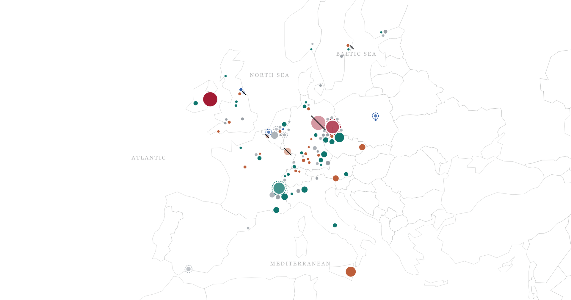
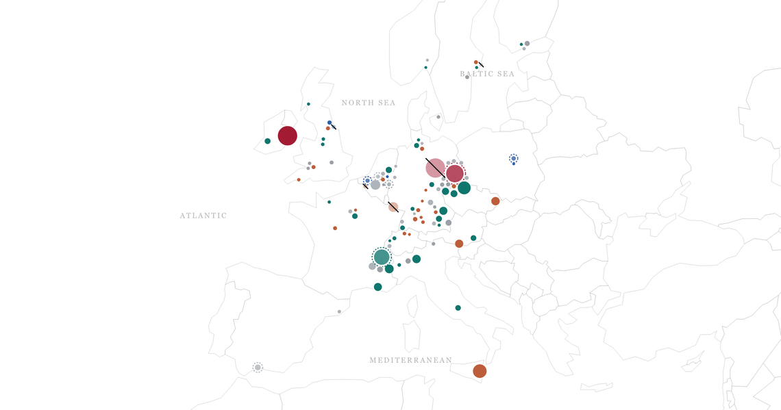
Search and filter 127 fab records in Europe: 74 chip fabs, 31 research lines and 22 wafer plants. Plus 44 back-end and 89 equipment sites.
Every site in the European Semiconductor Atlas: 127 fab records in 16 countries, 44 back-end sites and 89 equipment sites. Search and filter each table and download it as CSV. Updated 26 October 2026.
Jump to: Front-end wafer fabs · Back-end sites · Equipment makers · EU research grants
Click a row for details. The page address keeps your filters, so you can share a view.
Front-end wafer fabs
Colour:Leading-edge logicSiliconCompound semiconductorOther or unspecified materialWafer plantResearch or pilot lineStatus:Not yet in productionCancelled or closedShow on the map
| Company | Country | Status | Type | City | Finest node | Year | |
|---|---|---|---|---|---|---|---|
| Infineon TechnologiesVillach 300mm Thin-Wafer Power Fab (Innovation Fab) | Austria | Operational | Specialty | Villach | – | 2021 | |
| Infineon TechnologiesVillach 200mm SiC Fab (CoolSiC) | Austria | Operational | Compound semiconductor | Villach | – | 2025 | |
| Infineon TechnologiesVillach 200mm Silicon Power/Analog Fab (legacy) | Austria | Operational | Specialty | Villach | – | 2000 | |
| ams OSRAMPremstaetten 200mm specialty fab (full-service foundry) | Austria | Operational | Specialty | Premstaetten (Unterpremstaetten, Graz area) | 180 nm | 1983 | |
| ams OSRAMPremstaetten new front-end fab (European Chips Act) | Austria | Under construction | Specialty | Premstaetten (Unterpremstaetten, Graz area) | – | 2030 | |
| BelGaNOudenaarde Fab (ex-onsemi Fab2 / AMIS / Mietec) — BelGaN GaN line | Belgium | Cancelled | Compound semiconductor | Oudenaarde | 350 nm | 2022 | |
| Thema FoundriesOudenaarde Photonics Fab (ex-BelGaN site) | Belgium | Announced | Foundry | Oudenaarde | – | 2027 | |
| imecimec 300mm advanced CMOS R&D pilot line (Leuven) incl. NanoIC High-NA EUV extension | Belgium | Research pilot line | Leuven | 2 nm | 2026 | ||
| imecimec 200mm cleanroom (Leuven) | Belgium | Operational | Research pilot line | Leuven | – | – | |
| onsemiRožnov 150mm Silicon Power Device Fab | Czech Republic | Operational | Specialty | Rožnov pod Radhoštěm | 800 nm | 2003 | |
| onsemiRožnov Silicon & SiC Crystal Growth, Wafer & Epitaxy Operations | Czech Republic | Wafer plant | Rožnov pod Radhoštěm | n/a | – | ||
| onsemiRožnov Vertically Integrated SiC Device Fab (new end-to-end SiC line) | Czech Republic | Announced | Compound semiconductor | Rožnov pod Radhoštěm | – | 2027 | |
| Topsil GlobalWafersTopsil GlobalWafers Frederikssund (float-zone / NTD / CZ silicon wafers; FZ300 300mm R&D) | Denmark | Wafer plant | Frederikssund | n/a | 2027 | ||
| MurataVantaa MEMS Fab (ex-VTI Technologies) | Finland | Operational | Specialty | Vantaa | – | 1991 | |
| OkmeticVantaa Fab (existing 150/200mm line) | Finland | Operational | Wafer plant | Vantaa | n/a | 1997 | |
| OkmeticVantaa Fab Expansion (new 200mm fab, Koivuhaka) | Finland | Operational | Wafer plant | Vantaa | n/a | 2025 | |
| VTT / MicronovaMicronova Centre for Micro and Nanotechnology (incl. Kvanttinova RDI hub expansion) | Finland | Research pilot line | Espoo (Otaniemi) | – | 2026 | ||
| CEA-LetiCEA-Leti 200mm pilot line (CMOS + MEMS) | France | Operational | Research pilot line | Grenoble | – | not found | |
| CEA-LetiCEA-Leti 300mm silicon pilot platform (CMOS, photonics, 3D integration) | France | Operational | Research pilot line | Grenoble | not found | 2004 | |
| CEA-LetiFAMES Pilot Line (300mm, building 41.03) | France | Operational | Research pilot line | Grenoble | 7 nm | 2026 | |
| LIGENTECLIGENTEC France R&D Centre | France | Research pilot | Research pilot line | Corbeil-Essonnes | – | 2022 | |
| MACOM / OMMICMACOM European Semiconductor Center (former OMMIC III-V foundry) | France | Operational | Compound semiconductor | Limeil-Brevannes | 40 nm | – | |
| MurataCaen Silicon Capacitor / IPD Fab (Murata Integrated Passive Solutions, ex-IPDiA) | France | Specialty | Caen | – | 2024 | ||
| STMicroelectronicsCrolles 300mm | France | Logic | Crolles | 28 nm | 2003 | ||
| STMicroelectronicsCrolles 200mm | France | Operational | Logic | Crolles | 130 nm | – | |
| STMicroelectronicsRousset 200mm | France | Operational | Specialty | Rousset | 90 nm | 2000 | |
| STMicroelectronicsTours 200mm | France | Operational | Compound semiconductor | Tours | – | not found | |
| STMicroelectronics – GlobalFoundries JVCrolles 300mm ST-GlobalFoundries FD-SOI joint venture fab | France | Announced | Foundry | Crolles | 18 nm | 2026 | |
| SoitecBernin 1 (200mm SOI substrate fab) | France | Operational | Wafer plant | Bernin | n/a | 1999 | |
| SoitecBernin 2 (300mm SOI fab) | France | Operational | Wafer plant | Bernin | n/a | 2003 | |
| SoitecBernin 3 (POI substrate fab) | France | Operational | Wafer plant | Bernin | n/a | 2020 | |
| SoitecBernin 4 (SmartSiC SiC substrate plant) | France | Wafer plant | Bernin | n/a | 2024 | ||
| X-FABX-FAB France (Corbeil-Essonnes, former Altis Semiconductor) | France | Operational | Foundry | Corbeil-Essonnes | 110 nm | not found | |
| AZUR SPACE Solar PowerAZUR SPACE Heilbronn (Telefunken Technology Park) | Germany | Compound semiconductor | Heilbronn | – | 1964 | ||
| ESMC (TSMC + Bosch/Infineon/NXP JV)ESMC Dresden 300mm Fab | Germany | Under construction | Foundry | Dresden | 12 nm | 2028 exp. | |
| Ferdinand-Braun-Institut (FBH)FBH III-V Cleanroom (Cleanroom I & II) | Germany | Research pilot | Research pilot line | Berlin (Adlershof) | 100 nm | 1992 | |
| FraunhoferFraunhofer HHI Photonic InP Foundry / pilot line (Berlin) | Germany | Operational | Research pilot line | Berlin | – | – | |
| FraunhoferFraunhofer ENAS / Center for Microtechnologies (ZfM) cleanroom (Chemnitz) | Germany | Operational | Research pilot line | Chemnitz | – | – | |
| FraunhoferFraunhofer IPMS Center Nanoelectronic Technologies (CNT) 300mm CMOS R&D line (Dresden) | Germany | Operational | Research pilot line | Dresden | 22 nm | 2005 | |
| FraunhoferFraunhofer IPMS 200mm MEMS/MOEMS cleanroom (Dresden) | Germany | Operational | Research pilot line | Dresden | – | 2007 | |
| FraunhoferFraunhofer IPMS 200mm microdisplay / OLED-on-silicon cleanroom (Dresden) | Germany | Operational | Research pilot line | Dresden | – | 2008 | |
| FraunhoferFraunhofer IZM-ASSID 200/300mm 3D wafer-level integration pilot line (Dresden-Moritzburg) | Germany | Research pilot | Research pilot line | Dresden-Moritzburg | – | 2010 | |
| FraunhoferFraunhofer IMS 200mm CMOS line (Duisburg) | Germany | Operational | Research pilot line | Duisburg | 180 nm | – | |
| FraunhoferFraunhofer IISB pi-Fab silicon CMOS line (Erlangen, 200mm Si CMOS / 150mm HT-CMOS) | Germany | Research pilot | Research pilot line | Erlangen | – | not found | |
| FraunhoferFraunhofer IISB 150mm SiC power-device pilot line (Erlangen) | Germany | Operational | Research pilot line | Erlangen | – | not found | |
| FraunhoferFraunhofer IISB 200mm SiC line / demo lab (Erlangen, ramp-up) | Germany | Research pilot | Research pilot line | Erlangen | – | not found | |
| FraunhoferFraunhofer IAF III-V compound-semiconductor cleanroom / research fab (Freiburg) | Germany | Operational | Research pilot line | Freiburg im Breisgau | 50 nm | not found | |
| FraunhoferFraunhofer ISIT 200mm MEMS / power line (Itzehoe) | Germany | Operational | Research pilot line | Itzehoe | not found | 1995 | |
| FraunhoferFraunhofer EMFT Munich microelectronics/microsystems line (150mm MEMS + 200mm CMOS pilot, 3D integration) | Germany | Research pilot | Research pilot line | Munich | – | 2007 | |
| Freiberger Compound MaterialsFreiberg GaAs/InP/GaN substrate plant | Germany | Operational | Wafer plant | Freiberg | n/a | 1997 | |
| GlobalFoundriesDresden Fab 1 | Germany | Foundry | Dresden | 22 nm | 2009 | ||
| IHP (Leibniz)IHP 200mm SiGe BiCMOS Pilot Line | Germany | Research pilot | Research pilot line | Frankfurt (Oder) | 130 nm | 2021 | |
| Infineon TechnologiesDresden Wafer Fab (existing 200mm + 300mm) | Germany | Operational | Specialty | Dresden | – | 1995 | |
| Infineon TechnologiesSmart Power Fab Dresden (300mm, MEGAFAB-DD) | Germany | Operational | Specialty | Dresden | – | 2026 | |
| Infineon TechnologiesRegensburg Wafer Fab (150/200mm power & sensor) | Germany | Operational | Specialty | Regensburg | – | 2000 | |
| IntelMagdeburg Megafab (Silicon Junction) | Germany | Cancelled | Logic | Magdeburg | not found | – | |
| NexperiaNexperia Hamburg wafer fab | Germany | Specialty | Hamburg | – | 1953 | ||
| Robert BoschDresden Wafer Fab (300mm) | Germany | Specialty | Dresden | 65 nm | 2021 | ||
| Robert BoschReutlingen Wafer Fab (150mm/200mm) | Germany | Specialty | Reutlingen | 180 nm | 1970 | ||
| SiCrystal (ROHM)SiCrystal Nuremberg (Nordostpark) SiC substrate plant | Germany | Wafer plant | Nuremberg | n/a | 1997 | ||
| SiltronicBurghausen (crystal pulling + 300mm wafer fab, global tech/R&D center) | Germany | Operational | Wafer plant | Burghausen | n/a | 1998 | |
| SiltronicFreiberg 300mm fab (Carl-Schiffner-Strasse 29) | Germany | Operational | Wafer plant | Freiberg | n/a | 2004 | |
| TDK-MicronasFreiburg Wafer Fab | Germany | Operational | Specialty | Freiburg im Breisgau | not found | 1960 | |
| Q.ANTQ.ANT Thin-Film Lithium Niobate Photonic Pilot Line (at IMS CHIPS) | Germany | Research pilot | Research pilot line | Stuttgart | – | 2024 | |
| TRUMPF Photonic ComponentsUlm VCSEL & Photodiode Cleanroom (TRUMPF Photonic Components HQ) | Germany | Compound semiconductor | Ulm | – | 2008 | ||
| Texas InstrumentsFreising wafer fab (TI Deutschland) | Germany | Operational | Specialty | Freising | not found | 1976 | |
| United Monolithic Semiconductors (UMS)UMS Ulm GaAs/GaN-on-SiC MMIC Fab | Germany | Operational | Compound semiconductor | Ulm | 100 nm | not found | |
| Vishay IntertechnologyVishay Semiconductor Heilbronn wafer fab | Germany | Specialty | Heilbronn | – | – | ||
| Vishay IntertechnologySiliconix Itzehoe 200mm power fab | Germany | Operational | Specialty | Itzehoe | – | 1996 | |
| Vishay IntertechnologySiliconix Itzehoe 300mm power fab (new 12-inch) | Germany | Under construction | Specialty | Itzehoe | – | 2027 | |
| WolfspeedEnsdorf SiC Fab (Wolfspeed-ZF) | Germany | Cancelled | Compound semiconductor | Ensdorf | – | – | |
| X-FABX-FAB Dresden | Germany | Foundry | Dresden | 350 nm | – | ||
| X-FABX-FAB Erfurt (HQ) | Germany | Operational | Foundry | Erfurt | 110 nm | 1992 | |
| X-FABX-FAB MEMS Foundry Itzehoe | Germany | Operational | Foundry | Itzehoe | – | 2009 | |
| ams OSRAMRegensburg OSRAM Opto Semiconductors chip fab | Germany | Operational | Compound semiconductor | Regensburg | – | 2003 | |
| nanoplus Nanosystemsnanoplus Gerbrunn laser fab and group holding site | Germany | Operational | Compound semiconductor | Gerbrunn | – | 2001 | |
| nanoplus Nanosystemsnanoplus Meiningen laser fab and registered office | Germany | Operational | Compound semiconductor | Meiningen | – | 2009 | |
| Analog DevicesADI Limerick Wafer Fab (Raheen) | Ireland | Specialty | Limerick | 180 nm | 1977 | ||
| IntelFab 34 | Ireland | Operational | Logic | Leixlip | not found | 2023 | |
| IntelFab 24 (incl. Fab 24-2; legacy 200mm Fab 10/Fab 14 absorbed) | Ireland | Operational | Logic | Leixlip | 16 nm | 2006 | |
| LFoundryLFoundry Avezzano (200mm fab) | Italy | Operational | Foundry | Avezzano | 65 nm | 1990 | |
| MEMC / GlobalWafersMerano crystal growth plant (silicon single-crystal / ingots) | Italy | Operational | Wafer plant | Merano | n/a | 1976 | |
| MEMC / GlobalWafersNovara FAB300 (300mm) + legacy 150/200mm silicon wafer lines | Italy | Wafer plant | Novara | n/a | 2025 | ||
| STMicroelectronicsAgrate Brianza R3 300mm (AG300) | Italy | Specialty | Agrate Brianza | 90 nm | 2022 | ||
| STMicroelectronicsAgrate Brianza R3 300mm — Tower (TSIT) specialty foundry capacity | Italy | Operational | Foundry | Agrate Brianza | 65 nm | 2024 | |
| STMicroelectronicsAgrate Brianza 200mm (AG200) | Italy | Operational | Specialty | Agrate Brianza | – | – | |
| STMicroelectronicsCatania 150/200mm power & SiC/GaN device fab (existing) | Italy | Compound semiconductor | Catania | – | 1997 | ||
| STMicroelectronicsCatania Silicon Carbide Campus (200mm SiC device fab) | Italy | Operational | Compound semiconductor | Catania | – | 2026 | |
| STMicroelectronicsCatania SiC substrate and epiwafer plant | Italy | Wafer plant | Catania | n/a | 2026 exp. | ||
| Vishay IntertechnologyVishay Semiconductor Italiana wafer fab (Borgaro Torinese) | Italy | Operational | Specialty | Borgaro Torinese (Turin) | – | 1995 | |
| MESA+ Institute for Nanotechnology, University of TwenteMESA+ NanoLab cleanroom (NanoLabNL Twente) | Netherlands | Research pilot | Research pilot line | Enschede | 100 nm | 2010 | |
| NXP SemiconductorsNijmegen ICN8 | Netherlands | Operational | Specialty | Nijmegen | – | – | |
| SMART PhotonicsEindhoven InP PIC Foundry (High Tech Campus, 100mm line) | Netherlands | Operational | Foundry | Eindhoven | – | 2024 | |
| TNOEindhoven 6-inch InP Photonic Chip Pilot Line (PIXEurope, TNO-operated) | Netherlands | Under construction | Research pilot line | Eindhoven | – | 2027 exp. | |
| imecJoint imec-ASML High-NA EUV Lithography Lab (Veldhoven) | Netherlands | Research pilot | Research pilot line | Veldhoven | 2 nm | 2024 | |
| nanoPHAB B.VnanoPHAB nanophotonics micro-fab (NanoLab@TU/e) | Netherlands | Operational | Compound semiconductor | Eindhoven | – | 2015 | |
| SINTEFSINTEF MiNaLab (Micro- and Nanotechnology Laboratory) | Norway | Research pilot | Research pilot line | Oslo | – | 2004 | |
| Safran Sensing Norway ASHorten MEMS Fab (Sensonor / Safran Sensing Technologies Norway) | Norway | Operational | Specialty | Horten | – | 1985 | |
| VIGO PhotonicsOżarów Mazowiecki HQ fab (compound-semi epitaxy + IR detector line) | Poland | Operational | Compound semiconductor | Ożarów Mazowiecki | – | 2013 | |
| VIGO PhotonicsHyperPIC / MIRPIC mid-IR photonics foundry | Poland | Announced | Compound semiconductor | Ożarów Mazowiecki area (exact site not disclosed) | – | n/a | |
| Instituto de Microelectrónica de Barcelona , CSICIMB-CNM Integrated Micro and Nanofabrication Clean Room (Sala Blanca SBCNM, MICRONANOFABS node) | Spain | Operational | Research pilot line | Cerdanyola del Vallès (Bellaterra), Barcelona | – | 1991 | |
| imecimec 300mm R&D pilot line (Malaga / Andalusia) | Spain | Announced | Research pilot line | Malaga | – | n/a | |
| Coherent (ex-II-VI)Coherent Jarfalla 6-inch InP wafer fab | Sweden | Compound semiconductor | Jarfalla | – | not found | ||
| Coherent (ex-II-VI)Coherent Kista SiC substrate & epitaxy line (ex-Ascatron) | Sweden | Cancelled | Wafer plant | Kista, Stockholm | n/a | 2014 | |
| STMicroelectronicsNorrkoping SiC substrate and epiwafer fab (ex-Norstel) | Sweden | Operational | Wafer plant | Norrkoping | n/a | – | |
| Coherent (ex-II-VI)Coherent Zurich III-V laser fab (II-VI Laser Enterprise GmbH) | Switzerland | Operational | Compound semiconductor | Zurich | – | 1998 | |
| EM Microelectronic (Swatch)EM Microelectronic Marin Front-End Fab | Switzerland | Operational | Specialty | Marin-Epagnier (La Tene), Neuchatel | 180 nm | not found | |
| Hitachi EnergyLenzburg Power Semiconductor Front-End Fab (ex-ABB Semiconductors) | Switzerland | Operational | Specialty | Lenzburg | – | 1981 | |
| Hitachi EnergyHitachi Energy 300mm IGBT Wafer R&D / Pilot Line | Switzerland | Research pilot | Research pilot line | Lenzburg | – | not found | |
| LIGENTECLIGENTEC HQ / R&D and cleanroom (EPFL Innovation Park, Building L) | Switzerland | Research pilot | Research pilot line | Ecublens (Lausanne) | – | 2016 | |
| Safran TimingYverdon-les-Bains MEMS Fab (Colibrys / Safran Timing Technologies SA) | Switzerland | Operational | Foundry | Yverdon-les-Bains | – | – | |
| Octric SemiconductorsOctric Semiconductors Newton Aycliffe compound semiconductor fab | United Kingdom | Operational | Compound semiconductor | Newton Aycliffe, County Durham | – | – | |
| Diodes IncorporatedGreenock wafer fab (GFAB) | United Kingdom | Operational | Specialty | Greenock | – | not found | |
| Diodes IncorporatedOldham wafer fab (OFAB) | United Kingdom | Operational | Specialty | Oldham | – | 2008 | |
| IQEIQE Cardiff (St Mellons) — HQ epitaxy & Innovation Centre | United Kingdom | Operational | Wafer plant | Cardiff (St Mellons) | n/a | not found | |
| IQEIQE Milton Keynes (Tongwell) — Wafer Technology III-V substrates & epitaxy | United Kingdom | Operational | Wafer plant | Milton Keynes (Tongwell) | n/a | – | |
| IQEIQE Newport "Mega Foundry" (Imperial Park / Celtic Way, Coedkernew) | United Kingdom | Wafer plant | Newport (Coedkernew, Imperial Park) | n/a | 2018 | ||
| NexperiaNexperia Manchester (Hazel Grove) TrenchMOS wafer fab | United Kingdom | Operational | Specialty | Stockport (Hazel Grove), Greater Manchester | – | – | |
| Plessey SemiconductorsPlymouth Roborough Fab | United Kingdom | Operational | Compound semiconductor | Plymouth (Roborough) | not found | 1985 | |
| Pragmatic SemiconductorPragmatic Park (300mm FlexIC line) | United Kingdom | Operational | Specialty | Durham | 600 nm | 2024 | |
| Pragmatic SemiconductorNETPark Fab (200mm FlexIC line, legacy) | United Kingdom | Closed | Specialty | Sedgefield | 600 nm | 2018 | |
| Vishay IntertechnologyNewport Wafer Fab (Vishay Newport Limited) | United Kingdom | Operational | Specialty | Newport (Duffryn), South Wales | 180 nm | 1982 | |
| Silex MicrosystemsSilex MEMS Foundry, Järfälla | Sweden | Operational | Foundry | Järfälla | – | – | |
| Element 3-5Element 3-5 SiCnature SiC Epiwafer Plant | Germany | Announced | Wafer plant | Baesweiler | n/a | n/a | |
| KETEKKETEK Munich cleanroom (silicon drift detectors) | Germany | Specialty | Munich | – | 2008 | ||
| X-FABX-FAB Fab4Micro (MEMS open foundry), Erfurt | Germany | Under construction | Foundry | Erfurt | – | 2028 exp. | |
| SoitecHasselt GaN epitaxial wafer site | Belgium | Operational | Wafer plant | Hasselt | n/a | – |
n/a does not applynot found no published figure was found– not yet researchedWhat the atlas knows
Back-end sites: assembly, test and packaging
Colour:Merchant (OSAT)CaptiveResearch pilot lineStatus:Not yet in productionCancelled or closedShow on the map
| Company | Country | Access | Advanced packaging | City | Status | |
|---|---|---|---|---|---|---|
| Silicon Austria Labs (SAL) — FOWLP pilot line at SAL MicroFab, VillachSAL MicroFab, High Tech Campus Villach | Austria | Research pilot line | Wafer-level fan-out | Villach | Operational | |
| MelexisMelexis Ieper (headquarters/test/manufacturing site) | Belgium | Captive | None | Ieper (Ypres) | Operational | |
| imecimec Advanced Packaging / Chiplet Pilot Line (incl. NanoIC, FAMES) | Belgium | Research pilot line | 2.5D/3D, pilot | Leuven (Heverlee) | Research pilot | |
| MelexisMelexis Sofia (Melexis Bulgaria) | Bulgaria | Captive | None | Sofia | ||
| Sensata TechnologiesSensata Botevgrad (Sensata 3, formerly Sensor-Nite) | Bulgaria | Captive | None | Botevgrad | Operational | |
| Sensata TechnologiesSensata Maritsa/Tsaratsovo Plant (Plovdiv) | Bulgaria | Captive | None | Maritsa Municipality (near Tsaratsovo village), Plovdiv Region | Operational | |
| Hitachi Energy SemiconductorsHitachi Energy Semiconductors Prague | Czech Republic | Captive | None | Prague | Operational | |
| onsemi (ON Semiconductor)onsemi Rožnov pod Radhoštěm | Czech Republic | Captive | None | Rožnov pod Radhoštěm | ||
| Murata Electronics Oy (Murata Manufacturing)Murata Vantaa (Murata Electronics Oy technology center) | Finland | Captive | None | Vantaa | Operational | |
| Tampere University (SiPFAB) — Finnish Semiconductor Strategy / Chips JU WBG Pilot LineSiPFAB (System-in-Package Pilot Line), Tampere University, Hervanta Campus / Festia Building | Finland | Research pilot line | 2.5D/3D, pilot | Tampere | Under construction | |
| VTT Technical Research Centre of Finland (Micronova / Kvanttinova, APECS consortium partner)VTT Micronova / Kvanttinova (Espoo) - APECS pilot line | Finland | Research pilot line | 2.5D/3D, pilot | Espoo | Under construction | |
| CEA-LetiCEA-Leti FAMES Pilot Line (MINATEC Campus) | France | Research pilot line | 2.5D/3D, pilot | Grenoble | Operational | |
| STMicroelectronicsST Rennes | France | Captive | None | Rennes | Operational | |
| STMicroelectronicsST Tours (panel-level packaging pilot line) | France | Captive | 2.5D/3D, pilot | Tours | Under construction | |
| Fraunhofer ENAS (part of APECS / FMD pilot line)Fraunhofer Institute for Electronic Nano Systems ENAS, Chemnitz — APECS advanced packaging R&D pilot line | Germany | Research pilot line | 2.5D/3D, pilot | Chemnitz | Operational | |
| Fraunhofer IPMSFraunhofer IPMS Dresden – APECS 300mm Pilot Line (CEASAX / Center Nanoelectronic Technologies) | Germany | Research pilot line | 2.5D/3D, pilot | Dresden | Research pilot | |
| Fraunhofer IZM (Fraunhofer Institute for Reliability and Microintegration)Fraunhofer IZM - Wafer Level System Integration (WLSI), Berlin | Germany | Research pilot line | 2.5D/3D, pilot | Berlin | Operational | |
| Fraunhofer IZM-ASSID (All Silicon System Integration Dresden)Fraunhofer IZM-ASSID | Germany | Research pilot line | 2.5D/3D, pilot | Moritzburg (Dresden) | Operational | |
| GlobalFoundriesGlobalFoundries Dresden – Final Contacting (Bump and Sort) Facility | Germany | Captive | None | Dresden | Closed | |
| Infineon TechnologiesInfineon Regensburg (incl. Packaging Center Regensburg-Burgweinting) | Germany | Captive | 2.5D/3D, pilot | Regensburg | Operational | |
| Infineon TechnologiesInfineon Warstein | Germany | Captive | None | Warstein | Operational | |
| Melexis NVMelexis Erfurt | Germany | Captive | None | Erfurt | Operational | |
| Robert Bosch GmbH (Bosch Sensortec / Bosch Semiconductor)Bosch Reutlingen (wafer fab + on-site Test Center for Semiconductors) | Germany | Captive | None | Reutlingen | Operational | |
| Infineon TechnologiesInfineon Cegléd (Infineon Technologies Cegléd Kft. + Infineon Technologies Bipoláris Kft.) | Hungary | Captive | None | Cegléd | Operational | |
| Robert Bosch (Robert Bosch Elektronika Kft.)Bosch Hatvan – Final Test Center | Hungary | Captive | None | Hatvan | Operational | |
| SensirionSensirion Hungary Kft. Debrecen plant | Hungary | Captive | None | Debrecen | ||
| Tyndall National Institute (University College Cork)Tyndall National Institute — Photonic Packaging Group / Device Forensics (FlexiFab back-end) | Ireland | Research pilot line | 2.5D/3D, pilot | Cork | Operational | |
| IntelIntel Vigasio advanced packaging & assembly plant (planned) | Italy | Captive | None | Vigasio | Cancelled | |
| STMicroelectronicsSilicon Carbide Campus, Catania | Italy | Captive | None | Catania | Under construction | |
| STMicroelectronics | Italy | Captive | None | Marcianise | Operational | |
| Silicon BoxSilicon Box Novara | Italy | Merchant (OSAT) | 2.5D/3D, production | Novara (Agognate) | Announced | |
| STMicroelectronicsST Kirkop (STMicroelectronics Malta Ltd.) | Malta | Captive | None | Kirkop | Operational | |
| Sensonor AS (Safran Sensing Technologies Norway AS)Sensonor Horten MEMS manufacturing facility | Norway | Captive | None | Horten | Operational | |
| IntelIntel Wrocław (Miękinia) Semiconductor Integration and Test Facility — CANCELLED, never built | Poland | Captive | None | Wrocław (Miękinia commune) | Cancelled | |
| Amkor TechnologyAmkor Technology Portugal (ATEP) | Portugal | Merchant (OSAT) | Wafer-level fan-out | Vila do Conde | Operational | |
| KDPOF / KD (Knowledge Development for POF, S.L.)KD (KDPOF) Tres Cantos optoelectronic packaging and test facility | Spain | Captive | None | Tres Cantos, Madrid | ||
| Aptasic SAAptasic SA (Boudry HQ, now Eurofins Materials & Engineering Sciences) | Switzerland | Merchant (OSAT) | None | Boudry | Operational | |
| Hitachi Energy Semiconductors (formerly ABB Semiconductors)Hitachi Energy Semiconductors Lenzburg | Switzerland | Captive | None | Lenzburg | ||
| ALTER Technology (Alter Technology TÜV Nord)ALTER UK (ALTER Technology TÜV NORD UK Ltd, formerly Optocap) | United Kingdom | Merchant (OSAT) | None | Livingston, Scotland | Operational | |
| Compound Semiconductor Applications (CSA) CatapultCSA Catapult Innovation Centre — Advanced Packaging Prototype Facility / Power Packaging R&D Line | United Kingdom | Research pilot line | 2.5D/3D, pilot | Newport | Operational | |
| Custom Interconnect Ltd (CIL)Custom Interconnect Andover BP2 (Blueprint 2 OSAT facility) | United Kingdom | Merchant (OSAT) | 2.5D/3D, pilot | Andover | Operational | |
| Microchip TechnologyMicrochip Caldicot Advanced Packaging | United Kingdom | Captive | None | Caldicot | Operational | |
| Sivers Photonics (formerly CST Global)Sivers Photonics — Hamilton International Technology Park | United Kingdom | Merchant (OSAT) | None | Blantyre, South Lanarkshire (Glasgow area) | Operational | |
| Diodes Incorporated (Diodes Zetex Neuhaus GmbH)Diodes Neuhaus am Rennweg assembly and test | Germany | Captive | None | Neuhaus am Rennweg | Operational |
Equipment makers
Colour:Lithography and opticsDeposition, etch and thermalTest and metrologyVacuum, RF and laser partsBonding and packagingShow on the map
| Company | Country | Domain | City | Status | |
|---|---|---|---|---|---|
| BE Semiconductor Industries (Besi) — Besi Austria GmbH / Datacon Technology GmbHBesi Austria GmbH / Datacon Technology GmbH — Radfeld | Austria | Bonding and packaging | Radfeld | Operational | |
| EV Group (EVG)EV Group St. Florian am Inn (HQ, R&D and Manufacturing) | Austria | Bonding and packaging, Lithography, Metrology and inspection, Wet processing, Other | St. Florian am Inn | ||
| IMS Nanofabrication GmbHIMS Nanofabrication HQ / Manufacturing & R&D | Austria | Mask writing | Brunn am Gebirge | Operational | |
| ASM InternationalASM International Leuven (ASM Belgium NV) | Belgium | Deposition | Leuven | Operational | |
| Comet Group — Yxlon International A/S (Comet Technologies Denmark A/S)Yxlon International A/S (Comet Technologies Denmark A/S) — Taastrup plant | Denmark | Metrology and inspection | Taastrup | Operational | |
| ASM InternationalASM International Helsinki (Corporate R&D / ASM Microchemistry) | Finland | Deposition | Helsinki | Operational | |
| Picosun Oy (part of Applied Materials)Picosun Espoo (HQ / R&D) | Finland | Deposition | Espoo | Operational | |
| AnnealsysAnnealsys HQ / Manufacturing / R&D — Montpellier | France | Thermal, Deposition | Montpellier | Operational | |
| Laser Systems & Solutions of Europe SASU (LASSE)LASSE — Gennevilliers | France | Thermal | Gennevilliers | Operational | |
| MKS Instruments (Micro-Contrôle Spectra-Physics S.A.S / MKS Group)Micro-Contrôle Spectra-Physics — Beaune-la-Rolande plant | France | Lasers and optics, Metrology and inspection, Other | Beaune-la-Rolande | Operational | |
| MKS Instruments (Micro-Contrôle Spectra-Physics)MKS Instruments / Micro-Contrôle Spectra-Physics — Brigueuil manufacturing plant | France | Other | Brigueuil | Operational | |
| Pfeiffer VacuumPfeiffer Vacuum France (Annecy plant) | France | Vacuum and RF parts, Metrology and inspection | Annecy | Operational | |
| Plasma-Therm Europe SAS (CORIAL by Plasma-Therm, incl. Kobus)Plasma-Therm Europe / CORIAL Grenoble-Bernin Facility | France | Deposition, Etch | Bernin | Operational | |
| UnitySC (Unity Semiconductor SAS, part of Merck Group / Merck KGaA)UnitySC Global Headquarters | France | Metrology and inspection | Montbonnot-Saint-Martin | Operational | |
| 3D-Micromac AG3D-Micromac AG Headquarters and Production, Chemnitz | Germany | Lasers and optics, Other | Chemnitz | Operational | |
| ASMLASML Berlin (ex-Berliner Glas) | Germany | Lithography | Berlin | Operational | |
| AdvantestAdvantest Europe GmbH – Amerang | Germany | Test | Amerang | Operational | |
| Advantest | Germany | Test | Berlin | Operational | |
| AdvantestAdvantest Europe GmbH – Böblingen | Germany | Test | Böblingen | Operational | |
| Advantest | Germany | Test | Duisburg | Operational | |
| AdvantestAdvantest Europe GmbH (regional HQ) | Germany | Test | Munich | Operational | |
| AixtronAixtron Herzogenrath (HQ) | Germany | Deposition | Herzogenrath | Operational | |
| Busch Vacuum Solutions (Busch Group) — Busch Produktions GmbHBusch Produktions GmbH / Busch SE Headquarters, Maulburg | Germany | Vacuum and RF parts | Maulburg | Operational | |
| Carl Zeiss SMTCarl Zeiss SMT Coswig | Germany | Lithography | Coswig | Operational | |
| Carl Zeiss SMTCarl Zeiss SMT Jena | Germany | Mask writing, Metrology and inspection, Lasers and optics | Jena | Operational | |
| Carl Zeiss SMTCarl Zeiss SMT Wetzlar | Germany | Lithography | Wetzlar | Under construction | |
| Carl Zeiss SMT GmbHCarl Zeiss SMT Aachen | Germany | Lithography, Lasers and optics | Aachen | Operational | |
| Carl Zeiss SMT GmbHCarl Zeiss SMT Oberkochen (HQ) | Germany | Lithography, Lasers and optics | Oberkochen | Operational | |
| Carl Zeiss SMT GmbHCarl Zeiss SMT Rossdorf | Germany | Metrology and inspection, Other | Rossdorf | Operational | |
| Comet Group (Comet Yxlon GmbH / Comet Plasma Control Technologies)Comet PCT (Plasma Control Technologies) - RF Generator Center of Excellence | Germany | Other | Aachen | Operational | |
| Comet Group — Comet Yxlon GmbH (formerly Yxlon International GmbH)Comet Yxlon GmbH — Hamburg Headquarters, R&D & Manufacturing (IXS division) | Germany | Metrology and inspection | Hamburg | Operational | |
| ERS electronic GmbH | Germany | Bonding and packaging, Test, Metrology and inspection | Barbing (Regensburg) | Operational | |
| ERS electronic GmbHERS electronic GmbH HQ / Engineering Center / Production | Germany | Thermal, Test | Germering | Operational | |
| F&K Delvotec Bondtechnik GmbHF&K Delvotec Bondtechnik GmbH Headquarters | Germany | Bonding and packaging | Ottobrunn | Operational | |
| Finetech GmbH & Co. KG | Germany | Bonding and packaging | Berlin | Operational | |
| Heidelberg Instruments Mikrotechnik GmbHHeidelberg Instruments Mikrotechnik GmbH — HQ, Production & R&D Center (Wieblingen) | Germany | Mask writing, Lithography | Heidelberg | Operational | |
| Hesse GmbH (Hesse Mechatronics)Hesse GmbH Headquarters and Production, Paderborn | Germany | Bonding and packaging | Paderborn | ||
| Jenoptik AGJenoptik Airportpark Dresden micro-optics fab | Germany | Mask writing, Lasers and optics, Other | Dresden | Operational | |
| LPKF Laser & Electronics SELPKF Headquarters (Garbsen) | Germany | Lasers and optics, Etch, Other | Garbsen | Operational | |
| LayTec AGLayTec Headquarters and EpiX Manufacturing, Berlin | Germany | Metrology and inspection | Berlin | Operational | |
| Leybold GmbH (Atlas Copco)Leybold GmbH HQ | Germany | Vacuum and RF parts | Cologne | Operational | |
| Multiphoton Optics GmbH | Germany | Lithography | Würzburg | Operational | |
| Multitest Elektronische Systeme GmbH (now part of Cohu GmbH)Multitest Rosenheim plant | Germany | Test | Rosenheim | Operational | |
| Nanoscribe GmbH & Co. KGNanoscribe Headquarters (ZEISS Innovation Hub @ KIT Campus North) | Germany | Lithography, Mask writing | Eggenstein-Leopoldshafen (Karlsruhe) | Operational | |
| PVA TePla Analytical Systems GmbHPVA TePla Analytical Systems GmbH — Westhausen (SAM manufacturing/application center) | Germany | Metrology and inspection | Westhausen | Operational | |
| Pfeiffer VacuumPfeiffer Vacuum Dresden production site | Germany | Vacuum and RF parts | Dresden | Operational | |
| Pfeiffer VacuumPfeiffer Vacuum Components & Solutions GmbH (Pfeiffer Vacuum+Fab Solutions) — Göttingen production plant | Germany | Vacuum and RF parts | Göttingen | Operational | |
| Pfeiffer Vacuum GmbHPfeiffer Vacuum GmbH — HQ & Manufacturing (Asslar) | Germany | Vacuum and RF parts | Aßlar (Asslar) | Operational | |
| QuantumDiamonds GmbHQuantumDiamonds Munich (HQ/R&D at Fraunhoferstrasse 17; new production plant under construction in Weisses Quartier, eastern Munich) | Germany | Metrology and inspection | Munich | Under construction | |
| RENA Technologies GmbHRENA Technologies Headquarters and Main Production, Gütenbach | Germany | Wet processing | Gütenbach | Operational | |
| Raith GmbHRaith GmbH Headquarters (Phoenix West) | Germany | Lithography, Mask writing, Metrology and inspection | Dortmund | Operational | |
| Rasco GmbH (Cohu / Cohu GmbH)Rasco GmbH (Cohu GmbH), Kolbermoor plant | Germany | Test | Kolbermoor | Operational | |
| SENTECH Instruments GmbHSENTECH Instruments GmbH — Berlin-Adlershof HQ, R&D & Manufacturing | Germany | Etch, Deposition, Metrology and inspection | Berlin | Operational | |
| SUSS MicroTecSUSS MicroTec Garching (HQ) | Germany | Lithography, Deposition, Wet processing, Metrology and inspection, Bonding and packaging | Garching | Operational | |
| SUSS MicroTecSUSS MicroTec Sternenfels | Germany | Bonding and packaging, Lithography, Wet processing | Sternenfels | Operational | |
| TRUMPFTRUMPF Ditzingen (Group Headquarters) | Germany | Lasers and optics | Ditzingen | Operational | |
| TRUMPF Hüttinger GmbH + Co. KG (TRUMPF group)TRUMPF Hüttinger Freiburg | Germany | Vacuum and RF parts, Other | Freiburg im Breisgau | Operational | |
| VON ARDENNE GmbHVON ARDENNE Dresden (HQ, central production, Technology & Application Center) | Germany | Deposition | Dresden | Operational | |
| Vistec Electron Beam GmbHVistec Electron Beam GmbH — Jena plant | Germany | Mask writing, Lithography | Jena | Operational | |
| centrotherm international AGcentrotherm international AG — Blaubeuren HQ | Germany | Thermal, Deposition | Blaubeuren | Operational | |
| scia Systems GmbHscia Systems GmbH Headquarters / R&D / Manufacturing | Germany | Etch, Deposition | Chemnitz | Operational | |
| Semilab Semiconductor Physics Laboratory Zrt.Semilab Headquarters (Budapest) | Hungary | Metrology and inspection | Budapest | Operational | |
| LPE S.p.A. (ETC)LPE S.p.A. Baranzate plant (ETC) | Italy | Deposition | Baranzate (Milan) | Operational | |
| SPEA S.p.A.SPEA S.p.A. Headquarters & Manufacturing Plant | Italy | Test | Volpiano (TO) | Operational | |
| ASM InternationalASM International Almere (Versterkerstraat 8, HQ) | Netherlands | Deposition | Almere | Operational | |
| ASMLASML Global Headquarters / Veldhoven Campus | Netherlands | Lithography | Veldhoven | Operational | |
| ASML / imecASML-imec High-NA EUV Lithography Lab, Veldhoven | Netherlands | Lithography, Metrology and inspection | Veldhoven | Operational | |
| BE Semiconductor Industries (Besi)Besi Duiven (Besi Netherlands B.V. / Group HQ) | Netherlands | Bonding and packaging | Duiven | Operational | |
| Levitech BVLevitech Headquarters and Production | Netherlands | Deposition | Almere | Operational | |
| TRUMPF HüttingerTRUMPF Hüttinger Kobyłka (CTPark Warsaw East) | Poland | Other | Kobyłka | Operational | |
| TRUMPF HüttingerTRUMPF Huettinger Zielonka (Greater Warsaw) | Poland | Vacuum and RF parts | Zielonka | Operational | |
| Pfeiffer VacuumPfeiffer Vacuum Srl Production Plant Apahida | Romania | Vacuum and RF parts | Apahida (Cluj) | Operational | |
| VAT Group AG — VAT Romania SRLVAT Romania SRL — Arad (legacy plant: Str. I, Zona Industrială Arad Vest nr. 9; new plant: VGP Park Arad, DN 69 KM 46+215) | Romania | Vacuum and RF parts | Arad | Operational | |
| Sensofar-Tech, S.L. (Sensofar Metrology)Sensofar Metrology HQ / Manufacturing & R&D | Spain | Metrology and inspection | Terrassa | Operational | |
| Mycronic ABMycronic AB Headquarters / Pattern Generators Division, Täby | Sweden | Mask writing | Täby | Operational | |
| Obducat AB | Sweden | Lithography | Lund | Operational | |
| Attolight SAAttolight HQ / R&D-Manufacturing Site (EPFL Innovation Park) | Switzerland | Metrology and inspection | Lausanne (Ecublens) | Operational | |
| Carl Zeiss SMT (Carl Zeiss SMT Switzerland AG)Carl Zeiss SMT Zurich | Switzerland | Lithography, Other | Zurich | Operational | |
| Comet Group (Comet AG / Comet Holding AG)Comet AG Headquarters, Flamatt | Switzerland | Vacuum and RF parts, Metrology and inspection | Wünnewil-Flamatt | Operational | |
| Evatec AGEvatec AG Headquarters & Manufacturing Plant, Trübbach | Switzerland | Deposition | Trübbach | Operational | |
| Heidelberg Instruments Nano AG (formerly SwissLitho)Heidelberg Instruments Nano AG - Zurich (Bandliweg 30) | Switzerland | Lithography, Mask writing | Zurich | Operational | |
| VAT Group AG (VAT Vakuumventile AG)VAT Vakuumventile AG — Global HQ, Manufacturing & R&D | Switzerland | Vacuum and RF parts | Haag (Sennwald) | Operational | |
| Oxford Instruments Plasma TechnologyOxford Instruments Plasma Technology, Yatton | United Kingdom | Etch, Deposition | Yatton | Operational | |
| Plasma-Therm (Specialty Process Engineering Group)Plasma-Therm UK Ltd (Specialty Process Engineering Group) | United Kingdom | Etch, Deposition | Somerton | Operational | |
| SPTS Technologies (KLA Corporation)KLA SPTS Division R&D and Manufacturing Facility | United Kingdom | Etch, Deposition, Bonding and packaging | Newport | Operational | |
| memsstar Ltdmemsstar Ltd - Livingston (Kirkton Campus) | United Kingdom | Deposition, Etch | Livingston | Operational | |
| KLA (KLA-Tencor MIE GmbH)KLA-Tencor MIE GmbH, Weilburg | Germany | Metrology and inspection | Weilburg | Operational | |
| AixtronAixtron Cambridge | United Kingdom | Deposition | Cambridge | Operational | |
| AixtronAixtron Turin production site | Italy | Deposition | Turin | Operational |
What the columns mean
Each fab record has one type and four facets. The type names the kind of site. The facets say what the site makes and how.
- Type is one role per fab. If more than one role applies, the first match in this order wins: research or pilot line, wafer plant, foundry, compound semiconductor, memory, logic, specialty. A foundry makes chips that other companies design.
- Material is the semiconductor material of the devices: silicon (Si), silicon carbide (SiC), gallium nitride (GaN), gallium arsenide (GaAs), indium phosphide (InP) or other. GaN devices on silicon wafers count as GaN.
- Function is what the devices do: digital, memory, analog and mixed-signal, power, RF, sensing, optoelectronics or other. Sensing devices measure a quantity: motion, fields, pressure, images or radiation. Optoelectronic devices emit, guide or modulate light, or convert it to power.
- Form says how the maker builds the devices: integrated circuit, discrete, MEMS (small mechanical parts on a chip), passive or wafer. Lasers, LEDs and detector chips count as discrete devices. Wafer plants have the form "Wafer" and no function.
- Process is the manufacturing process family of the fab, as in the processes post. A fab can run more than one. Click a process to read how it works.
- An empty facet means that the sources do not say. The atlas does not guess a value from the type. The one exception is silicon for logic, specialty and memory fabs.
- Finest node records a published nominal node or minimum feature dimension in nanometres. Node names are process labels, not a directly comparable transistor dimension. Branded process names remain in the details when no numeric dimension is published; scanner wavelength is excluded. Many specialty fabs do not publish a node.
- Year is the year the fab opened. "Exp." marks the year in which a new fab expects to start production.
- Investment is the published cost of the fab. Public funding shows one principal recorded funding item, linked to its evidence and labelled by instrument and scope. Operator/project and shared programme amounts have no sourced site allocation. They, repayable loans, mixed grant/tax aid without a grant-only split and public investment commitments are excluded from site grant totals. A Commission state-aid approval concerns national aid, not an EU grant. Approval does not mean payment.
- Status uses the atlas words: announced, under construction, operational, expanding, research pilot, closed and cancelled.
For the back-end sites, Access says who the site works for. A merchant site, or OSAT (outsourced assembly and test), works for other companies. A captive site packages chips for its owner. Advanced packaging names the most advanced method at the site: wafer-level fan-out, flip-chip or stacked 2.5D/3D packaging.
For the equipment makers, Domain is the kind of machine or part. Sole supplier marks a manufacturing site associated with a sole supplier of a specified machine or part. It does not establish that every production step occurs exclusively at that site. Roles says if the site makes products, does research and development (R&D) or holds the headquarters.
The processes post explains how the manufacturing processes behind these facets differ. About the Atlas gives the sourcing rules.
What the atlas knows
An empty cell can mean three different things, and the tables keep them apart. "n/a" means that the field does not apply. A wafer plant has no node, and a fab that is not open has no opening year. "Not found" means that a search on the date in the CSV found no published figure. A dash means that the atlas has not researched the field yet.
This table counts the 127 fab records for each field.
| Field | Known | Not found | Not applicable | Not yet researched |
|---|---|---|---|---|
| Year opened | 87 | 14 | 6 | 20 |
| Employees | 79 | 19 | 0 | 29 |
| Investment | 60 | 36 | 0 | 31 |
| Capacity | 34 | 66 | 0 | 27 |
| Finest node | 34 | 7 | 22 | 64 |
Of the 44 back-end sites, 34 have an employee count and 31 have an opening year. Of the 89 equipment sites, 44 have an employee count and 22 have an opening year.
To report an error, use the "Report a correction" link in the details of a row. You can also write to kontakt@richard-stahl.at. I apply corrections and credit the sender.
EU research grants by operator
The European Commission publishes every grant of its Horizon research programmes in CORDIS. This table adds up the EU contribution for 54 operators in the atlas, from Horizon 2020 (2014 to 2020) and Horizon Europe (from 2021).
- EU chip programmes counts the projects of the EU joint undertakings for chips: ECSEL (2014 to 2020), Key Digital Technologies (2021 to 2023) and the Chips Joint Undertaking (from 2024). The member states also pay a share of these projects. The table shows only the EU share.
- The All Horizon grants column counts every Horizon grant to the operator, in any field. It includes the chip programmes.
Grants go to legal entities, not to fabs. The table has one row for each operator and does not show the grants for a site. Some legal entities do much more than chips, and the note names these cases. For example, the CEA total covers CEA as a whole, not only CEA-Leti. A group total also includes the entities of the group outside Europe.
The column "Public funding" in the fab table shows a different measure: recorded national aid, EU pilot-line grants and separately labelled shared programme amounts or loans. Part of the pilot-line money is in both counts, because the partners' Horizon share is also in CORDIS. Do not add the two together. Fab projects groups site grant approvals by status and lists selected projects; it is not a complete funding register.
| Operator | EU chip programmes, €m | All Horizon grants, €m | Projects | Note |
|---|---|---|---|---|
| imec | 594.5 | 876.2 | 505 | |
| CEA-Leti | 338.6 | 1,331.6 | 1277 | All of CEA, not only Leti |
| Fraunhofer | 145.2 | 1,264.5 | 1871 | All Fraunhofer institutes |
| Infineon Technologies | 134.0 | 192.4 | 165 | |
| STMicroelectronics | 119.9 | 158.2 | 163 | |
| ASML | 59.4 | 59.4 | 25 | |
| Carl Zeiss SMT | 38.4 | 38.7 | 12 | |
| Soitec | 35.8 | 38.9 | 33 | |
| VTT / Micronova | 34.3 | 529.7 | 772 | |
| NXP Semiconductors | 32.8 | 48.1 | 82 | |
| Robert Bosch | 27.1 | 94.9 | 165 | The whole Bosch group (all fields) |
| Instituto de Microelectrónica de Barcelona, CSIC | 11.3 | 799.6 | 1786 | All of CSIC |
| MESA+ Institute for Nanotechnology, University of Twente | 10.5 | 261.8 | 421 | All of the University of Twente |
| X-FAB | 8.7 | 12.7 | 20 | |
| Besi | 5.0 | 6.0 | 17 | |
| IHP (Leibniz) | 4.8 | 39.0 | 54 | |
| Aixtron | 4.6 | 21.9 | 28 | |
| GlobalFoundries | 4.5 | 5.4 | 11 | |
| ams OSRAM | 3.5 | 8.9 | 18 | |
| SINTEF | 3.2 | 334.5 | 468 | |
| LIGENTEC | 3.2 | 10.5 | 20 | |
| BelGaN | 3.1 | 5.0 | 5 | |
| Siltronic | 3.1 | 3.1 | 11 | |
| SMART Photonics | 3.0 | 11.6 | 19 | |
| Murata | 2.5 | 3.2 | 14 | |
| United Monolithic Semiconductors (UMS) | 1.9 | 2.6 | 7 | |
| TRUMPF | 1.7 | 3.4 | 6 | |
| Okmetic | 1.7 | 1.7 | 12 | |
| Coherent (ex-II-VI) | 1.4 | 5.0 | 13 | |
| Freiberger Compound Materials | 1.1 | 1.3 | 4 | |
| Nexperia | 1.0 | 1.5 | 9 | |
| Silex Microsystems | 0.9 | 3.9 | 5 | |
| LFoundry | 0.6 | 1.0 | 6 | |
| ASM International | 0.5 | 0.5 | 3 | |
| Analog Devices | 0.4 | 2.2 | 10 | |
| onsemi | 0.2 | 0.2 | 3 | |
| Intel | 0.1 | 23.3 | 60 | All Intel entities in the grant data, also in Israel and the US |
| KETEK | 0.1 | 0.1 | 1 | |
| Vishay Intertechnology | 0.1 | 0.1 | 1 | |
| Ferdinand-Braun-Institut (FBH) | 0 | 67.4 | 118 | All Forschungsverbund Berlin institutes |
| VIGO Photonics | 0 | 5.9 | 15 | |
| nanoplus Nanosystems | 0 | 5.6 | 7 | |
| MACOM / OMMIC | 0 | 3.6 | 7 | |
| AZUR SPACE Solar Power | 0 | 3.3 | 6 | |
| Pragmatic Semiconductor | 0 | 3.0 | 9 | |
| IQE | 0 | 1.4 | 7 | |
| Safran Timing | 0 | 0.8 | 1 | |
| Topsil GlobalWafers | 0 | 0.7 | 3 | |
| Plessey Semiconductors | 0 | 0.5 | 1 | |
| MEMC / GlobalWafers | 0 | 0.4 | 1 | |
| nanoPHAB B.V | 0 | 0.2 | 1 | |
| Q.ANT | 0 | 0.2 | 1 | |
| Texas Instruments | 0 | less than 0.1 | 1 | |
| TRUMPF Photonic Components | less than 0.1 | less than 0.1 | 1 |
The table includes only the operators that the search found in CORDIS. An operator that is not in the table got no Horizon grant, or uses a legal name that the search does not cover. The source is CORDIS open data, as of 2 October 2026 (© European Union, CC BY 4.0). The file eu-grants.json names the legal entities behind each total. The project-level funding ledger lists the participant records used to audit the aggregates. Totals sum CORDIS ecContribution; the ledger also retains netEcContribution, which can differ. These are recorded contributions, not evidence of cash payments.
Data date and licence
The data was last updated on 26 October 2026. The research snapshot is from June 2026 for the fabs and from July 2026 for the back-end and equipment sites. In October 2026 I checked the fab projects and many other fab records again, as Europe's Chip Fab Projects describes. Every record carries its sources. The tables show the first source of each record and a direct source for its recorded public funding.
The atlas is open data under CC BY 4.0. Please credit it as "European Semiconductor Atlas, richard-stahl.at". The full files have every source and the coordinates: fabs as CSV, fabs as GeoJSON, back-end sites as GeoJSON, equipment sites as GeoJSON and EU research grants as JSON.
More from the atlas
- The interactive map shows the same sites on a map of Europe.
- Who Makes Europe's Chips profiles the companies behind the sites.
- Europe's Chip Fab Projects shows which new fab projects opened, which are still in construction and which stopped.
Thinking out loud, by email
Occasional notes on technology, Europe, and whatever else has my attention. No spam — unsubscribe anytime.





Member discussion